SATSAGEN INTERFACE

Franck F1SSF has produced an interesting PCB that collects all functions and schematics of the USBDAALBFER interface project (Video).

Franck's SATSAGEN INTERFACE REV. E
Franck’s SATSAGEN INTERFACE REV. E


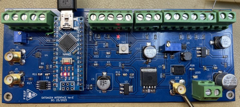
With SATSAGEN and Franck’s PCB, you can:


Download the Gerber files here or contact Franck F1SSF, but his PCB availability is limited.

Download the Arduino sketch here to compile and upload it to the interface.


Follow Franck’s instruction steps to wire and make operational his SATSAGEN INTERFACE PCB:

Hi All, Some information here. This PCBA is the first realization:

  • Inserted components except Nano and resistors 0U:
    • Use IBom:
  • Power UP:
    • Power supply on 12V IN connector
  • ADF5355 power supply
    • Measure R10 pad = 6V, if OK solder R10=0U
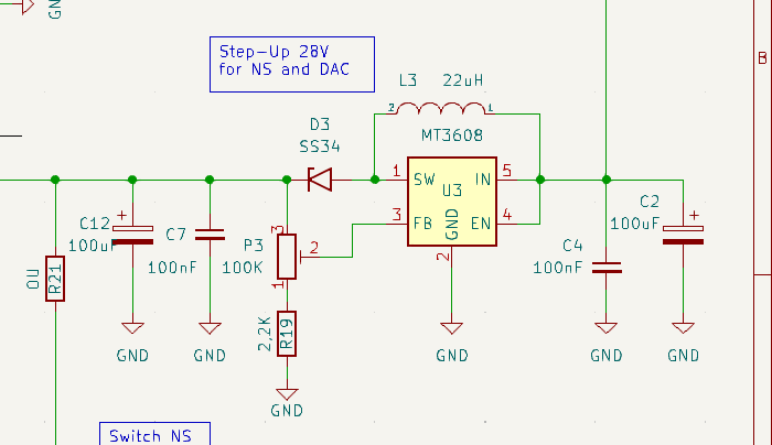
  • Step Up 28V – Warning, add modify R19 as below picture
    • Measure R23 pad, adjust P3 to obtain 28V max, If OK solder R23=0
  • Detector Step Up = ON:
    • Measure divider R2/R3, you must have 3Vmax
  • +15V DAC
    • Measure R13 pad = 15V, if OK solder R13=0U
  • Power OFF
  • Solder wires directly on serial chip Arduino (see schematic for pin numbers)
    • Plug Arduino on support for removal easily, and solder wires DCD = TP1, RI=TP2
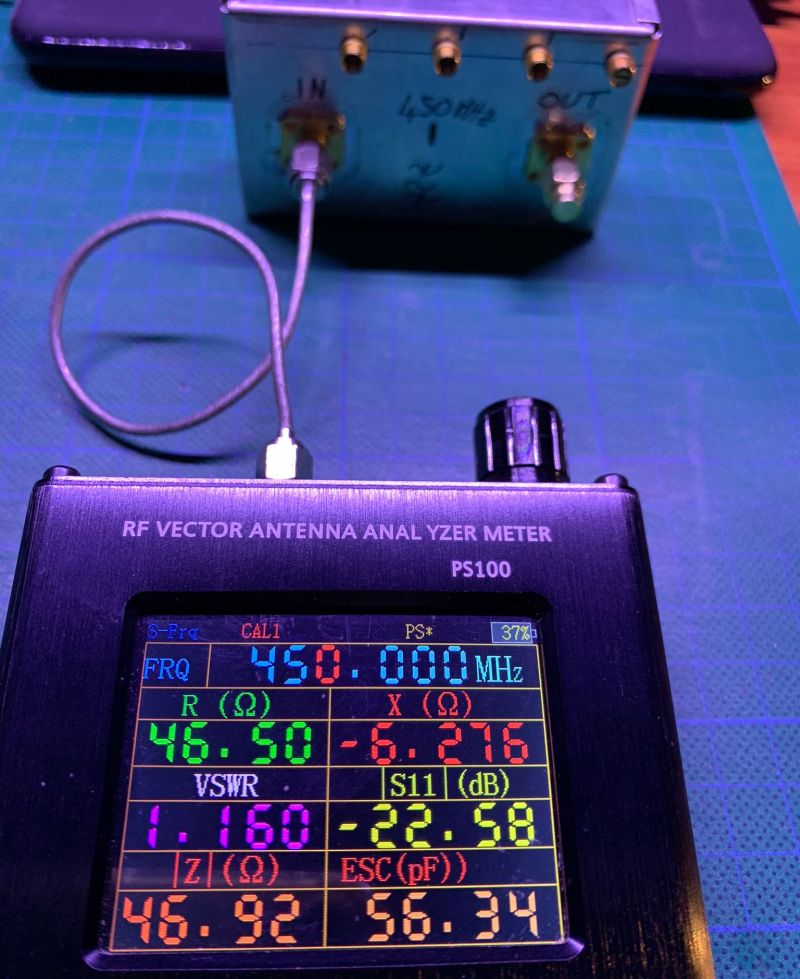
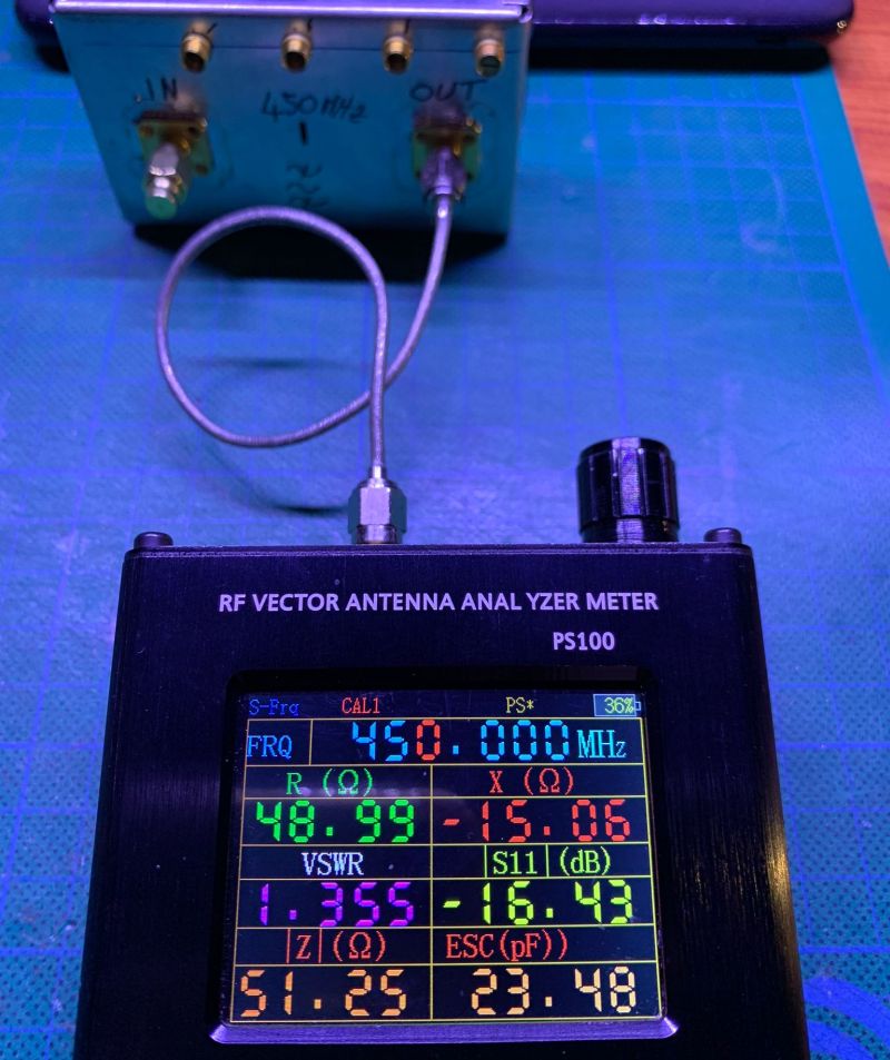
  • Check the values of the ADF5355 voltage dividers
    • R12/R22. R16/R24. R18/R25
  • Now you can connect all peripherals
    • Use connectors J6 , J11, J5, J7, J10
  • +3V ref
    • Adjust P4 to have +3V on Arduino pin ref N°18
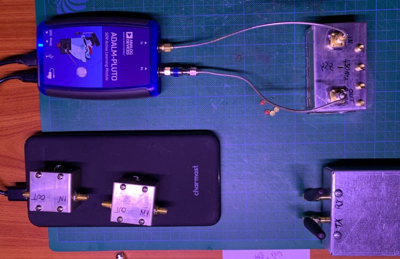
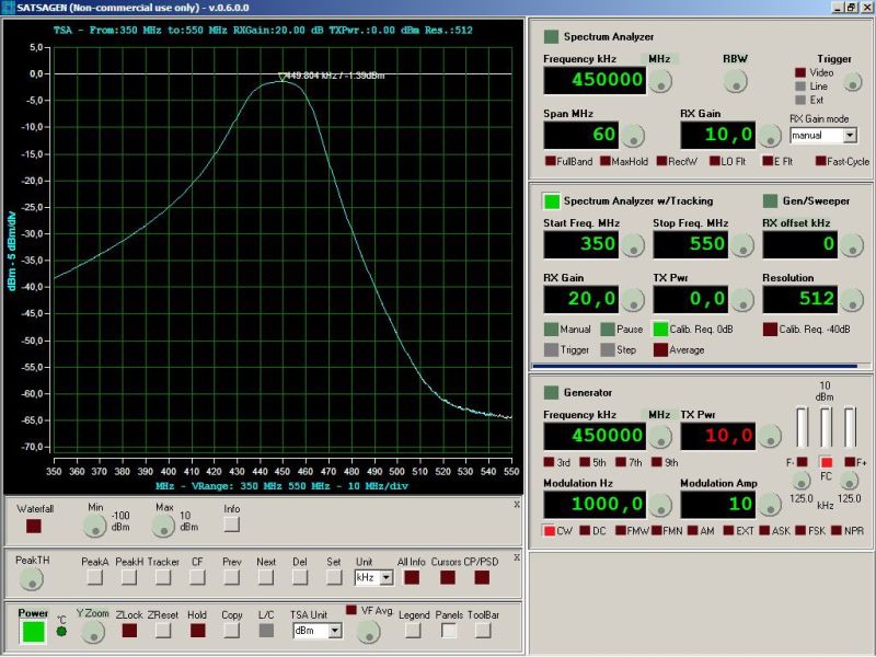
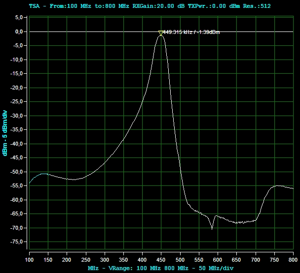
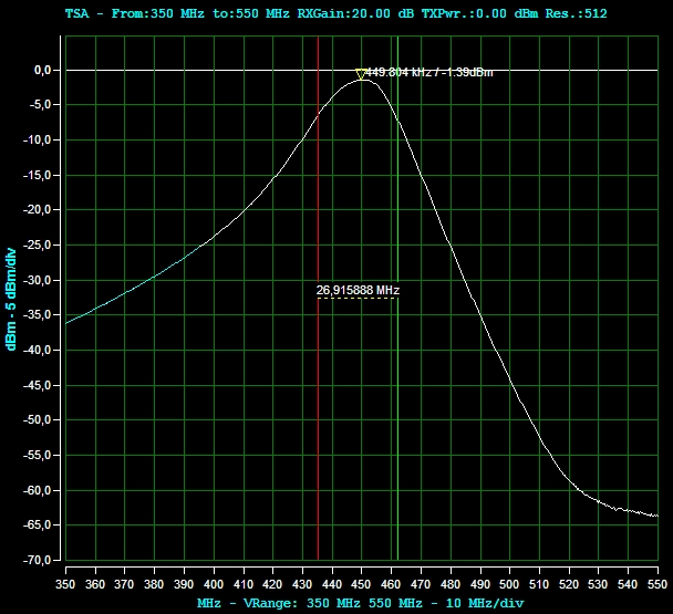
  • Configure Satsagen in tracking mode 0 to 6Ghz
    • See on J3 voltage ramp from 0V to about 12V.

SW1 allows you to select the operating modes of the Arduino, depending on the use.

You can deport SW1, LED1, and LED3 on the front end with J11 and J9.

If you move the LEDs, then remove the SMD LEDs or if you leave them, then change the R6 and R22 to adapt the current. SW1 can stay on board.

J1 / J2 / J10 Footprints are BNC connectors, but you can use SMA connectors after cutting legs. You solder ground around directly around the body.

Because the ADF5355 consumes approximately 200mA, it is recommended not to exceed 12V power supply to reduce the dissipation of the 6V regulator. I added a small radiator with thermal glue.

If your RF switch HMC536 already contains 100U resistors on ports A and B under the shield, replace R34 and R35 with 0U.

73’s  Franck F1SSF

Franck’s Satsagen Interface schematic Rev E-01

MT3608 step-up 28 Volts section schematic with the R19 to add

The 2k2 R19 to add

The 6 V regulator with a small radiator

450 MHz Band Pass Filter

Luigi IZ7PDX made this filter. It is a bandpass centered at 450 MHz that Luigi will use as an IF filter.

Luigi IZ7PDX’s centered bandpass filter at 450MHz front panel view.
The filter inside without the notch section activated (“parked” at 580 MHz).

Luigi characterized the filter using ADALM-PLUTO and SATSAGEN.

It’s the setup for the analysis of the filter. Note the attenuator placed on the RX side to improve impedance matching and preserve the RX stage of ADALM-PLUTO from possible damage.
The resulting response curve in a span of 200 MHz. The insertion loss is around 1.3 dB
It’s a scan performed with a 700MHz span.

Luigi has further improved the input and output impedance of the filter by acting on the coupling links and measuring with a vector antenna Analyzer:

It is scanning with a span of 200 MHz after improving the in/out impedance of the filter. The filter is “narrower” in terms of bandwidth than the previous scan before intervening on the coupling links.

Find Luigi IZ7PDX on:
- Youtube channel
- Site

GPSDO

This equipment is a precise clock generator, able to provide programmable frequencies from 8KHz to 200MHz on three independent outputs.

The generation of the signals is provided by a Si5351A. In this application, the Si5351A PLL uses as a reference a disciplined oscillator (GPSDO) based on the G7020-KT chip.

The control of GPSDO, PLL and the user interface (a 101X80 pixel color LCD and an encoder) is provided by an ATMega328P operating at 3.3V-8MHz.

Power is supplied by a 3.7V 600mA lpo battery which guarantees about four hours of use. The battery is connected to the step-up module which provides 5V for some modules and 3.3V through two LDOs via a CPU-controlled mosfet switch; the use of the mosfet guarantees the switching off of the appliance if the battery level drops. This switch circuit allows to have a quiescent current close to 0 uA. The charge and discharge control of the battery is also provided by the CPU and the TP4056/DW01A chips for charging and the overcharge protection and in additional overdischarge protection in the event of a CPU lock. The battery level is constantly displayed on the LCD, both during discharge and charging phases.

The “heart” of the generator is a VCTCXO oscillator which provides the reference to the G7020-KT GPS module and the Si5351A. The control voltage of the VCTCXO is given by a MCP4725 DAC (12bit resolution and I2C interface). The values ​​sent to the DAC are processed by the CPU based on the feedback received from the GPS module about the offset of the reference oscillator with respect to the one hooked to the satellite. The CPU receives UBX messages about the Drift clock from the G7020-KT via a serial connection. The DAC is equipped with an internal EEPROM memory that allows the sending of the control voltage preset to VCTCXO at moment of power-up, to speed up the GPS syncronize.

From the user interface it is possible to set the frequencies and power levels of the three outputs of the Si5351, respectively with a resolution of 1Hz and with four different output levels; 0.76DBm, 7DBm, 10DBm and 12DBm. The equipment has also a fourth output in SMA, concerning the PPS output of the GPS module synthesizer, also this last output is programmable from the user interface in frequency from 1Hz to 24MHz (for an acceptable phase noise, use only 48MHz sub-multiples) and in duty cycle from 1% to 99%. It is possible to set the PPS active only during the GNSS sync, moreover it is also possible to set manually the value sent to the DAC, a useful function for example to speed up calibration in the event of VCTCXO replacement.

All the above settings can be saved in the EEPROM of the CPU so that after a few seconds from a subsequent restart, the equipment generates the frequencies with the saved settings.

The yellow LED on the panel shows the PPS output signal negate (LED off = high signal), while the green LED indicates the correction operation performed on the VCTCXO: LED off = no GPS reception or PDO higher than 5 (minimum level to consider the clock drift), LED flashing = tDOP less than 5, clock drift above +/- 4ns and a correction of the VCTCXO voltage by the DAC is in progress, LED on steady = clock drift below +/- 5ns.

Finally, the following dynamically updated values ​​are displayed on the GPS screen: number of satellites used, the DOP (time dilution of precision), the clock drift value expressed in ns (corresponding to an oscillator deviation of 0.026 Hz per unit ), the type of fixed none, 2D or 3D, the position in longitude and latitude and meters above sea level, date and time in UTC, and finally the value of the voltage sent by the DAC to the VCTCXO in the range from 0 to 4095 (in steps of about 0.8mv); the VCTCXO responds to the control voltage in a negative way, so as the voltage rises the frequency of the VCTCXO drops.